4 Best Practices for Effective Electronics Board Design in Medical Devices
Introduction Creating printed circuit boards (PCBs) for medical devices is a complex...


The world of medical device design relies heavily on the precision of printed circuit board (PCB) layouts, where even the smallest error can lead to significant consequences. As healthcare technology evolves, grasping best practices in PCB design is crucial for ensuring safety, compliance, and performance. Designers encounter various challenges in navigating the regulatory landscape while pursuing innovation. It is essential to implement strategies that not only meet established standards but also enhance the reliability of medical devices.
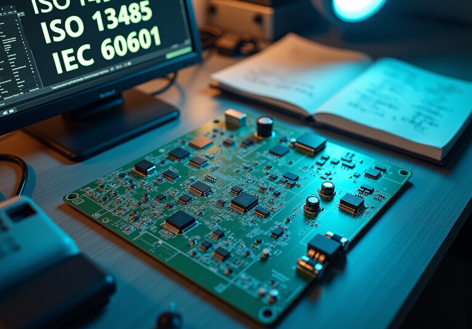
In the creation of healthcare equipment, adherence to regulatory standards is paramount. Designers must possess a thorough understanding of standards such as ISO 13485, IEC 60601, and FDA regulations, which govern the safety, performance, and quality management systems for medical devices. The FDA's Quality Management System Regulation (QMSR) delineates the necessary documentation and testing procedures that must be adhered to throughout the creation and manufacturing processes.
To ensure compliance, PCB designers should integrate these standards into their PCB layouts from the outset, conducting regular audits and reviews to verify adherence. This proactive approach not only facilitates regulatory approvals but also significantly enhances the reliability and safety of the medical products being developed.
Moreover, it is crucial to identify common pitfalls in establishing manufacturing evaluations, such as inadequate documentation or insufficient protocols, which can lead to costly delays and compliance issues. By implementing best practices in testing and quality assurance, manufacturers can effectively navigate these challenges and ensure that their electronic products meet the requisite standards efficiently.

A structured process for PCB layouts is crucial for the successful development of medical devices and encompasses several key steps:
This methodical approach serves as a best practice, ensuring timely completion and adherence to budget constraints.
Begin by developing a comprehensive schematic that accurately represents the circuit's functionality, serving as the blueprint for the entire project. Following this, strategically place components in the PCB layouts to minimize trace lengths and optimize signal integrity, which is vital for maintaining performance in high-frequency applications.
Once placement is complete, route the connections in the PCB layouts while adhering to guidelines regarding trace width and spacing, ensuring compliance with standards such as IEC 60601-1 and ISO 13485. Employ layout rule checks (DRCs) to identify potential issues early in the process, as common mistakes can result in costly revisions and delays.
Engaging with PCB producers early in the planning phase can further enhance compliance and optimize the design of PCB layouts for manufacturability. Finally, conduct a thorough review of the PCB layouts to ensure they meet all regulatory and performance requirements. This structured method not only enhances the reliability of the product but also streamlines the transition to manufacturing, significantly reducing the likelihood of issues during production.

Enhancing pcb layouts for healthcare equipment involves applying specific methods, such as:
Effective thermal management strategies, such as thermal vias and heat sinks, are critical in preventing component overheating, which significantly impacts reliability. Furthermore, simulation tools are essential for predicting performance issues before manufacturing, allowing for necessary adjustments that improve signal integrity and overall functionality. For instance, multi-layer configurations can optimize routing efficiency and minimize the board's footprint, which is particularly advantageous in compact healthcare instruments. By prioritizing these optimization techniques, designers can create PCB layouts that not only meet but also exceed performance expectations, ensuring compliance with stringent regulatory standards and enhancing patient safety.

A comprehensive evaluation and verification of PCB layouts are essential to ensure the reliability and safety of healthcare instruments. This process should incorporate several methodologies:
Initially, visual inspections can identify any apparent defects. Following this, ICT verifies that all components are correctly placed and operational, with a significant percentage of medical devices passing this test on the first attempt, highlighting its effectiveness. Functional evaluation assesses PCB layouts' performance under real-world conditions, confirming that they meet all specified requirements.
Applying Design for Testability (DFT) principles can further enhance evaluation and debugging processes. By establishing a comprehensive testing protocol that includes AOI, designers can improve quality assurance, ensuring compliance with regulatory standards and ultimately leading to safer medical devices. AOI, for instance, plays a pivotal role in identifying defects early in the manufacturing process, significantly reducing costs associated with corrections and improving overall product quality.

Ensuring the highest standards in PCB layouts for medical device design is not merely a regulatory requirement; it is a critical factor in safeguarding patient health. By integrating compliance with standards such as ISO 13485, IEC 60601, and FDA regulations into the design process, PCB designers can enhance the reliability and safety of medical devices from the outset. This proactive approach is essential for navigating the complexities of regulatory approvals and ensuring that products meet stringent performance criteria.
The article outlines several best practices pivotal in achieving successful PCB layouts. These include:
Each step, from initial schematic creation to thorough testing protocols, contributes to a comprehensive workflow that minimizes risks and ensures compliance with industry standards. Emphasizing the importance of early engagement with PCB producers and the application of design for testability principles further solidifies the pathway to creating safe and effective medical devices.
In conclusion, the significance of meticulous PCB layout design in the medical field cannot be overstated. Adopting these best practices not only streamlines the development process but also plays a vital role in enhancing patient safety and product reliability. Stakeholders in the medical device industry are encouraged to prioritize these guidelines, as they represent a commitment to excellence in design and a proactive stance against potential compliance issues. By doing so, they contribute to a future where medical devices are not only innovative but also safe and effective for all users.
Why is regulatory compliance important in PCB layout design for healthcare equipment?
Regulatory compliance is crucial because it ensures the safety, performance, and quality management of medical devices, adhering to standards such as ISO 13485, IEC 60601, and FDA regulations.
What are some key regulatory standards that PCB designers must understand?
PCB designers must understand standards including ISO 13485, IEC 60601, and FDA regulations, which govern the creation and manufacturing of medical devices.
What does the FDA's Quality Management System Regulation (QMSR) require?
The QMSR outlines the necessary documentation and testing procedures that must be followed throughout the creation and manufacturing processes of medical devices.
How can PCB designers ensure compliance with regulatory standards?
PCB designers can ensure compliance by integrating regulatory standards into their layouts from the beginning and conducting regular audits and reviews to verify adherence.
What benefits does a proactive compliance approach provide?
A proactive approach facilitates regulatory approvals and significantly enhances the reliability and safety of the medical products being developed.
What are common pitfalls in establishing manufacturing evaluations?
Common pitfalls include inadequate documentation and insufficient protocols, which can lead to costly delays and compliance issues.
How can manufacturers navigate challenges in regulatory compliance?
Manufacturers can navigate challenges by implementing best practices in testing and quality assurance to ensure their electronic products meet the requisite standards efficiently.
Do you have a question about our services, pricing, samples, resources, or anything else?
