4 Best Practices for Ensuring Signal Integrity in PCB Design
Discover best practices for ensuring signal integrity in PCB design for reliable...


Printed circuit board (PCB) design is fundamental to modern electronics, influencing everything from consumer gadgets to critical medical devices. As the demand for advanced electronic solutions surges, understanding the principles of PCB design becomes paramount, offering insights into optimizing performance, reliability, and compliance. Engineers face significant challenges in adapting to rapid technological advancements and increasing complexity in electronic devices. This necessitates a proactive approach to design that not only meets current standards but also anticipates future needs.
The development of printed circuit boards (PCBs) is a critical process that underpins the functionality of modern electronic devices. In 2026, approximately 90% of digital devices will utilize PCB layout in their production, demonstrating its widespread application in various sectors, including consumer electronics and healthcare. A PCB assembly employs copper conductors to connect diverse electronic components, facilitating their communication and functionality. The development process includes several stages, such as:
All focused on optimizing electrical connections for improved performance and reliability. Significantly, the medical device sector depends extensively on PCB architecture, with biocompatible and sterile PCBs being essential for implantable devices, ensuring safety and longevity. Successful PCB development projects in consumer electronics further illustrate its versatility, as seen in award-winning products showcased at CES 2026, where innovations like LG Display’s 27-inch 4K RGB-stripe OLED panel exemplified the importance of advanced PCB technologies.
Industry leaders stress that effective PCB creation is vital for balancing performance, cost, yield, and manufacturability, making it a crucial element in the development of modern technology. At Voler Systems, we focus on professional electronic creation services for medical equipment, utilizing AI-assisted engineering to expedite the advancement of wearable and IoT solutions. With extensive experience in developing medical instruments such as heart pumps and liquid biopsy platforms, we deliver high-quality solutions that meet healthcare's stringent requirements.
Moreover, our emphasis on enhancing battery longevity in wireless medical equipment through ultra-low power approaches exemplifies our dedication to innovation. Engineers at Voler Systems are trained to plan effectively, evaluate project feasibility, and intervene when necessary, ensuring that all technological projects are completed on time and within budget. This comprehensive method not only boosts the reliability of our creations but also emphasizes the significance of test systems in preserving quality and performance in electronic device development. Ultimately, the success of technological advancements hinges on the effectiveness of PCB design and assembly.

The journey of PCB development began in the early 20th century, marked by significant innovations that transformed electronic design and manufacturing. Austrian engineer Paul Eisler created the first functional PCB in 1936 for a radio, marking a definitive transition from traditional point-to-point wiring methods to a more compact and efficient structure. By the 1960s, the introduction of multilayer PCBs revolutionized the industry, enabling the integration of more complex circuits within a smaller footprint. This advancement was essential for the miniaturization of devices, which gained importance in the rapidly growing consumer technology market.
Throughout the decades, significant advancements in materials and manufacturing processes have propelled what is PCB design to new capabilities. The development of surface mount technology (SMT) in the late 1980s and 1990s allowed components to be mounted directly onto the surface of PCBs, eliminating the need for drilled holes and enhancing circuit density. Automation in PCB manufacturing further streamlined production, reducing costs and improving accuracy.
Today, PCBs are essential to nearly all digital devices, from smartphones to advanced medical equipment, highlighting their vital role in technological advancement. The multilayer PCB market, valued at approximately $71 billion in 2023, is projected to grow at a CAGR of 5.5% from 2024 to 2032, driven by the increasing demand for compact and efficient electronic solutions. As the demand for advanced electronic solutions continues to rise, knowing what is PCB design will remain a cornerstone of innovation in the industry.

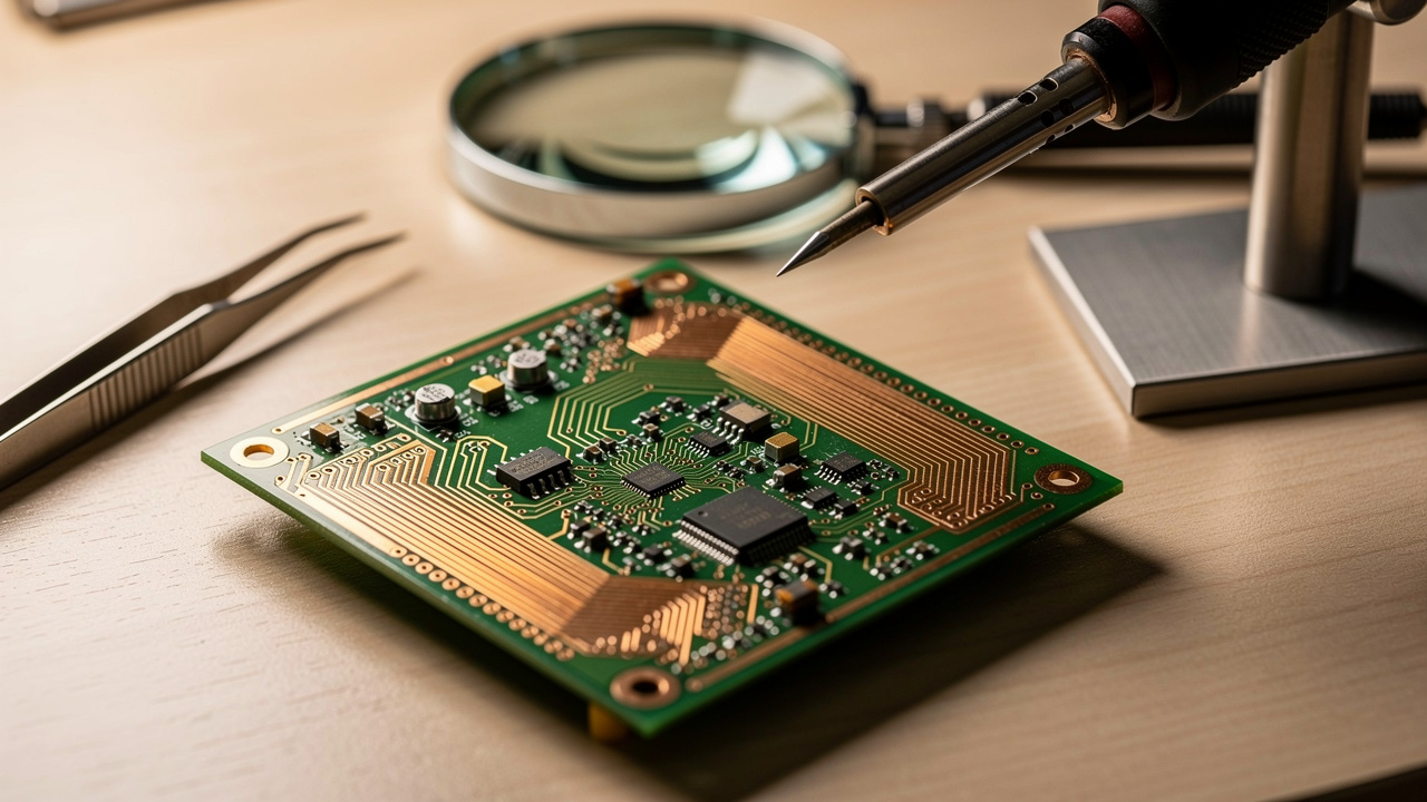
Understanding what is PCB design is essential, as the creation of printed circuit boards (PCBs) hinges on several key elements that directly impact their functionality and reliability. Key components include the substrate, conductive traces, pads, and vias.
Effective arrangement of these elements is critical; for instance, the dielectric constant of the substrate significantly influences signal fidelity, thermal stability, and overall product cost. Engineers stress that the choice of substrate material is paramount, as it directly affects the performance of the PCB. A recent case study demonstrated that optimizing conductive trace layout improved functionality by reducing interference by 25%, thereby enhancing overall reliability.
Understanding what is PCB design and the interplay among these components is crucial for the development of high-performance PCBs that satisfy the rigorous demands of contemporary electronics.

What is PCB design, and why is it a foundational element in electronics that influences both reliability and performance in critical applications? A well-designed PCB reduces the likelihood of electrical failures, enhances signal integrity, and ensures compliance with regulatory standards, particularly in sensitive areas such as medical equipment. Voler Systems ensures that its medical equipment formulations meet emissions and ESD requirements, adhering to standards such as ISO 13485. This compliance is essential for guaranteeing patient safety and equipment efficacy. Their innovative approach to embedded systems development leverages FPGA and AI technologies, optimizing battery life and performance in wireless medical devices.
Understanding what is PCB design is crucial as effective PCB layout reduces manufacturing errors and improves yield rates, leading to significant cost savings. The growing complexity of electronic devices underscores the need for engineers to prioritize understanding what is PCB design in their development processes.

PCB design is not merely a technical skill; it is a foundational element that drives the functionality of modern electronic devices. As the backbone of virtually all digital technology, understanding PCB design is essential for anyone involved in electronics. A thorough understanding of PCB design enhances device performance and reliability while ensuring compliance with industry standards, especially in critical areas like medical equipment.
Throughout this article, we have explored key concepts surrounding PCB design, including:
The journey from early innovations to today's advanced multilayer PCBs highlights the ongoing importance of this field, while the emphasis on precision in design and the use of cutting-edge technologies showcases how PCB design continues to shape the future of electronics.
Reflecting on PCB design reveals its crucial role in fostering innovation across multiple sectors. For engineers and designers, prioritizing a deep understanding of PCB design principles is not just beneficial but necessary for developing reliable, efficient, and compliant electronic solutions. This commitment to understanding PCB design principles directly translates into superior product outcomes and technological advancements.
What is PCB design, and why is it important?
PCB design involves creating printed circuit boards that are essential for the functionality of modern electronic devices. It is important because approximately 90% of digital devices will utilize PCB layout in their production by 2026, impacting various sectors, including consumer electronics and healthcare.
What are the core stages involved in the PCB development process?
The core stages in the PCB development process include schematic capture, layout creation, and routing. These stages focus on optimizing electrical connections for improved performance and reliability.
How are PCBs used in the medical device sector?
In the medical device sector, PCBs are crucial as they need to be biocompatible and sterile for implantable devices, ensuring safety and longevity.
Can you provide an example of PCB innovation in consumer electronics?
An example of PCB innovation in consumer electronics is LG Display’s 27-inch 4K RGB-stripe OLED panel, which was showcased at CES 2026 as an award-winning product highlighting advanced PCB technologies.
What factors do industry leaders consider important in PCB creation?
Industry leaders emphasize the importance of balancing performance, cost, yield, and manufacturability in PCB creation, making it a crucial element in the development of modern technology.
What services does Voler Systems provide in relation to PCB design?
Voler Systems offers professional electronic creation services for medical equipment, utilizing AI-assisted engineering to expedite the development of wearable and IoT solutions.
What experience does Voler Systems have in developing medical instruments?
Voler Systems has extensive experience in developing medical instruments such as heart pumps and liquid biopsy platforms, delivering high-quality solutions that meet stringent healthcare requirements.
How does Voler Systems enhance battery longevity in medical equipment?
Voler Systems enhances battery longevity in wireless medical equipment through ultra-low power approaches, demonstrating their dedication to innovation.
What is the significance of test systems in electronic device development?
Test systems are significant in electronic device development as they help preserve quality and performance, ensuring the reliability of technological projects.
Do you have a question about our services, pricing, samples, resources, or anything else?
