Introduction
Signal integrity is paramount in PCB design, especially for high-speed applications where data accuracy is essential. Designers encounter significant obstacles in ensuring signal clarity due to factors such as:
- Crosstalk
- Ground bounce
- Impedance mismatches
This article explores best practices that enhance signal integrity in printed circuit boards while safeguarding against pitfalls that may compromise device functionality, particularly in sensitive fields like medical technology. Engineers must navigate these complexities to ensure the reliability and efficiency of their designs.
Understand Signal Integrity and Its Importance in PCB Design
Signal integrity in PCB design plays a pivotal role, especially for high-speed digital and analog transmissions, as it influences the quality of an electrical pulse during its passage through a circuit. Poor transmission quality can result in significant issues, including data loss, increased error rates, and system failures, particularly detrimental in medical device applications where precision is essential.
Factors that negatively impact transmission integrity include:
- Crosstalk
- Ground bounce
- Impedance mismatches
For instance, crosstalk occurs when neighboring conductors allow energy coupling from one trace to another, leading to unintended interference. Ground bounce, which arises from excessive current consumption, can alter the circuit's reference level, resulting in fluctuating ground voltage levels that compromise transmission quality. Additionally, impedance mismatches can cause reflections, further degrading the transmission.
Recognizing these factors allows designers to adopt effective strategies that guarantee signal integrity in PCB and ensure reliable communication between components. For example:
- Maintaining uniform trace widths and spacing
- Utilizing low-loss PCB materials
- Employing daisy chain routing
These strategies can significantly enhance signal integrity in PCB. Moreover, incorporating decoupling capacitors near power pins can stabilize voltage levels and mitigate ground bounce.
Voler Systems excels in embedded systems development, applying AI-driven engineering to enhance power management and extend battery life, which is crucial in wireless medical equipment. With expertise spanning Class I to Class III medical devices, wearables, IoT, and consumer electronics development, Voler Systems ensures compliance with safety standards like IEC 60601-1 while maintaining device performance. This commitment to excellence ensures that our solutions not only meet but exceed industry standards, fostering trust in critical medical applications.

Implement Key Design Considerations for Optimal Signal Integrity
To ensure optimal signal integrity in PCB design, it is crucial to implement several key considerations that reflect best practices in engineering design projects:
- Trace Length and Routing: Keep traces as short and direct as possible to minimize delay and distortion. Routing sensitive information on internal layers close to reference planes significantly reduces noise exposure and enhances overall performance. Avoid routing high-speed transmissions through multiple connectors or vias, as improper routing can lead to significant signal degradation, impacting overall system performance.
- Controlled Impedance: Implement controlled impedance traces to match the impedance of the source and load, which minimizes reflections. This practice is especially vital for high-speed transmissions, where mismatches can result in considerable degradation.
- Layer Stack-Up: Careful planning of the layer stack-up is essential. Ensure that power and ground planes are adjacent to communication layers to provide a solid reference and reduce electromagnetic interference (EMI), which can negatively impact data quality. Larger boards should be designed with consideration for trace lengths to mitigate the risk of crosstalk and EMI.
- Termination: Proper termination techniques should be employed to match the impedance at the end of the transmission line. This helps prevent reflections that may disrupt data quality, especially in high-speed applications.
- Grounding: Utilize a solid ground plane to provide a low-impedance return path for transmissions. This is essential for preserving transmission quality, as it reduces the possibility of crosstalk and EMI, ensuring dependable operation of the PCB. Additionally, place decoupling capacitors near power pins to stabilize power supply voltages and reduce noise.
- Simulation tools should be utilized to analyze signal integrity in PCB and evaluate the effect of physical arrangement on performance. These tools can assist in recognizing potential problems early in the creation process, enabling prompt modifications.
Incorporating these best practices will enhance the reliability and performance of PCBs in medical device applications. Neglecting these best practices could compromise the reliability of PCBs, ultimately affecting the success of medical device development projects.

Manage Noise and Interference to Enhance Signal Integrity
Noise and interference pose significant challenges to achieving signal integrity in PCB designs. To effectively manage these issues, consider the following strategies:
- Separation of Types: Physically isolate high-speed digital transmissions from low-frequency analog communications to minimize crosstalk and interference. This separation reduces the risk of high-frequency waves affecting delicate analog circuits.
- Shielding: Employ shielding techniques, such as enclosing sensitive components in grounded metal enclosures or using custom shielding cans and gaskets, to protect against external electromagnetic interference (EMI). A well-designed stack-up can act as a natural shield against EMI, enhancing the overall performance of the PCB.
- Decoupling Capacitors: Position decoupling capacitors close to the power pins of integrated circuits (ICs) to eliminate high-frequency noise and maintain stable voltage levels. This practice is crucial for ensuring stable power delivery and reliable device operation.
- Grounding Techniques: Implement distinct ground planes for analog and digital circuits to prevent digital switching noise from impacting sensitive analog data. Proper grounding techniques are essential for preserving signal integrity in PCB and minimizing EMI.
- Trace Routing: Avoid running traces parallel to each other over long distances, as this can induce crosstalk. Instead, utilize staggered routing or ground traces to minimize interference. Additionally, minimizing via count on high-speed traces helps avoid impedance discontinuities. Keeping current loop areas small and ensuring well-defined return paths are also critical for reducing unintended emissions.
- EMI Pre-Compliance Testing: Perform EMI pre-compliance testing whenever feasible to identify potential issues early in the development process. This proactive approach can prevent costly redesigns and troubleshooting later on.
By adopting these strategies, designers can ensure their PCBs meet the demands of modern electronic applications.

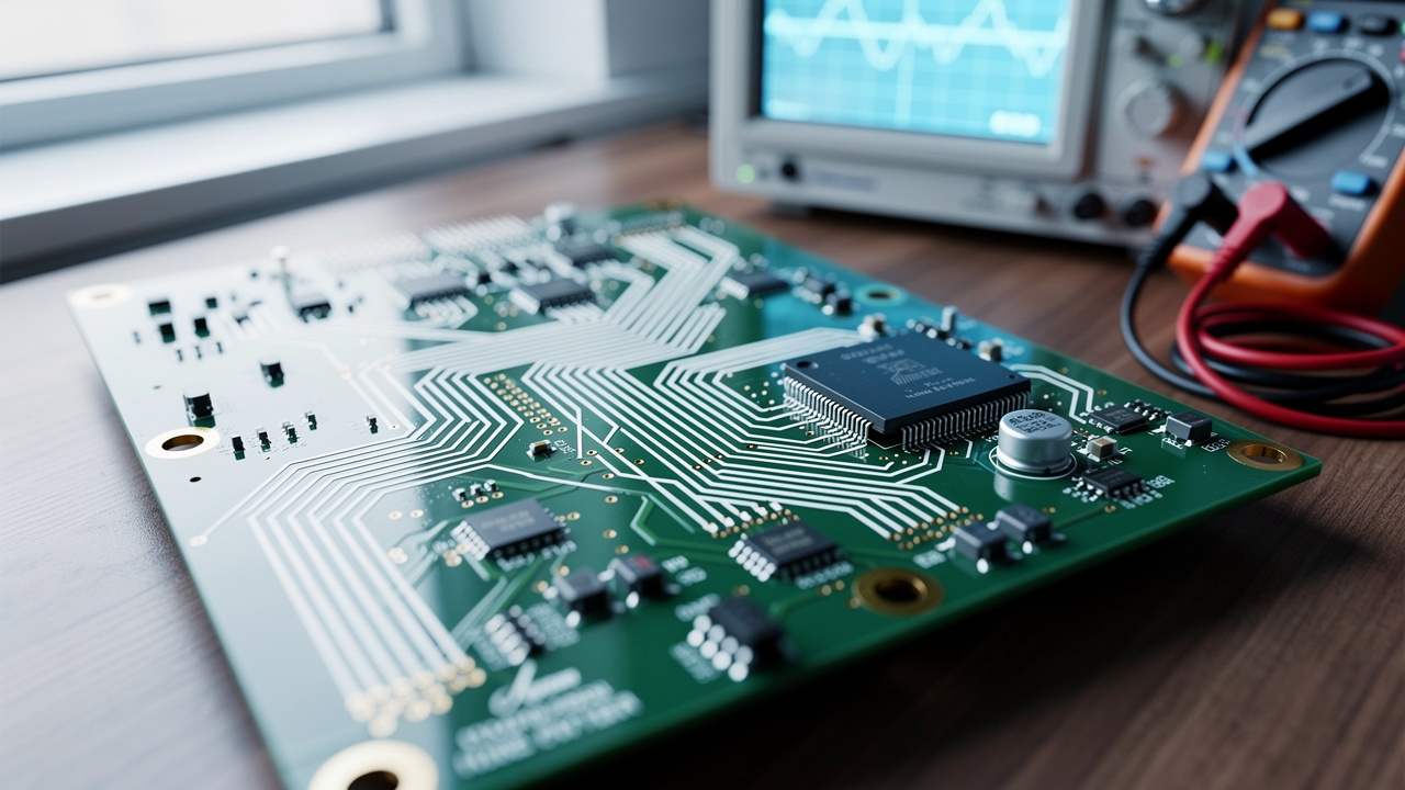
Test and Validate Designs to Ensure Signal Integrity
Ensuring signal integrity in PCB layouts is critical, especially for wearable sensors and wireless medical devices. Key methods include:
- Simulation Tools: Utilize simulation software to examine waveform integrity during the creation phase. Tools like SPICE can forecast behavior in the final product, addressing potential issues before physical prototyping. Each design stage necessitates specific capabilities from simulation tools, such as speed or accuracy, particularly as data rates and simulation complexity increase.
- Time-Domain Reflectometry (TDR): Utilize TDR to measure impedance and identify reflections in the transmission path. Impedance mismatches can lead to significant transmission degradation, complicating the design process. This method enables modifications to occur prior to production, ensuring that data quality is maintained and reducing the likelihood of mistakes in high-speed applications.
- Oscilloscope Measurements: Conduct real-time measurements with oscilloscopes to observe waveforms. Oscilloscopes offer timing, jitter, and level information for comprehensive integrity assessments, assisting in identifying problems like ringing or distortion, which can greatly affect performance, particularly in medical equipment where dependability is crucial. These measurements are critical for optimizing device performance in wearable technology.
- Eye Diagrams: Analyze eye diagrams to evaluate the quality of digital transmissions. This approach offers understanding of timing and data quality, enabling engineers to see possible issues that might influence data transmission rates, which are becoming more crucial as applications require faster speeds. Voler Systems leverages AI-driven engineering to optimize these assessments, ensuring robust data communication.
- Post-Layout Verification: Execute post-layout analysis to detect any problems introduced during the layout procedure. Most signal integrity analysis is performed by full-time specialists, but there are far too few specialists for the number of PCBs being designed. This step is crucial for guaranteeing that the final blueprint meets all performance standards, particularly in settings with stringent regulatory compliance obligations, such as maintaining signal integrity in PCB for medical equipment manufacturing. This rigorous approach not only enhances performance but also aligns with the stringent demands of the medical device industry.

Conclusion
Neglecting signal integrity in PCB design can jeopardize the reliability and performance of electronic devices, especially in high-speed applications. Understanding critical factors affecting signal quality - such as crosstalk, ground bounce, and impedance mismatches - enables designers to implement strategies that enhance communication between components and prevent costly failures.
Throughout the article, key practices have been highlighted, including:
- Maintaining uniform trace widths
- Implementing controlled impedance
- Utilizing effective grounding techniques
The importance of simulation tools and testing methods, such as Time-Domain Reflectometry and oscilloscopes, has been emphasized as a vital step in validating designs to ensure optimal signal integrity. These measures are crucial in medical devices, where precision and reliability are essential.
Ultimately, adopting these best practices not only improves signal integrity but also fosters greater confidence in the performance of PCBs across various applications. Designers are encouraged to prioritize these strategies to mitigate risks and enhance the reliability of their products. Prioritizing these strategies not only mitigates risks but also positions designers as leaders in the evolving landscape of medical device technology.
Frequently Asked Questions
What is signal integrity in PCB design?
Signal integrity in PCB design refers to the quality of an electrical pulse as it travels through a circuit, which is crucial for high-speed digital and analog transmissions.
Why is signal integrity important?
Signal integrity is important because poor transmission quality can lead to data loss, increased error rates, and system failures, which are particularly critical in applications like medical devices where precision is essential.
What factors negatively impact signal integrity?
Factors that negatively impact signal integrity include crosstalk, ground bounce, and impedance mismatches.
What is crosstalk?
Crosstalk occurs when neighboring conductors allow energy coupling from one trace to another, resulting in unintended interference.
What is ground bounce?
Ground bounce arises from excessive current consumption, altering the circuit's reference level and causing fluctuating ground voltage levels that compromise transmission quality.
How do impedance mismatches affect signal integrity?
Impedance mismatches can cause reflections in the signal, which further degrades transmission quality.
What strategies can be adopted to ensure signal integrity?
Effective strategies include maintaining uniform trace widths and spacing, utilizing low-loss PCB materials, employing daisy chain routing, and incorporating decoupling capacitors near power pins to stabilize voltage levels.
How does Voler Systems contribute to signal integrity in PCB design?
Voler Systems excels in embedded systems development, applying AI-driven engineering to enhance power management and extend battery life, which is vital for wireless medical equipment, while ensuring compliance with safety standards.
What types of devices does Voler Systems specialize in?
Voler Systems specializes in a range of devices including Class I to Class III medical devices, wearables, IoT, and consumer electronics.
What is the significance of Voler Systems' expertise in medical device development?
Voler Systems' expertise in medical device development ensures compliance with safety standards like IEC 60601-1 while maintaining device performance, fostering trust in critical medical applications.
List of Sources
- Understand Signal Integrity and Its Importance in PCB Design
- pcdandf.com (https://pcdandf.com/pcdesign/index.php/editorial/menu-features/18330-managing-signal-integrity-in-high-speed-pcbs)
- protoexpress.com (https://protoexpress.com/blog/signal-integrity-issues-in-pcb)
- analog.com (https://analog.com/en/resources/technical-articles/dont-get-zapped.html)
- designnews.com (https://designnews.com/electronics/headline-designcon-2026-showcases-breakthroughs-in-signal-integrity-high-speed-interconnect-technologies)
- bench.com (https://bench.com/setting-the-benchmark/enhancing-medical-device-reliability-in-signal-intense-settings)
- Implement Key Design Considerations for Optimal Signal Integrity
- ecadstar.com (https://ecadstar.com/en/blog/signal-integrity)
- pcbpower.us (https://pcbpower.us/blog/pcb-trace-length-matching-high-speed-design)
- allpcb.com (https://allpcb.com/allelectrohub/the-impact-of-standard-pcb-dimensions-on-signal-integrity-what-you-need-to-know)
- actalentservices.com (https://actalentservices.com/en/insights/articles/how-to-manage-signal-integrity-and-emi-in-pcb-design)
- foxtronicsems.com (https://foxtronicsems.com/pcba-manufacturing/pcb-assembly-trends-oems-need-to-know-in-2026)
- Manage Noise and Interference to Enhance Signal Integrity
- camptechii.com (https://camptechii.com/practical-emi-control-in-pcb-design)
- researchgate.net (https://researchgate.net/publication/372302552_Direct-write_shielded_cables_for_improved_signal_integrity)
- resources.altium.com (https://resources.altium.com/p/emi-emc-design-pcb-noise-reduction-through-isolation-of-ac-and-dc-signals)
- protoexpress.com (https://protoexpress.com/blog/7-pcb-design-tips-solve-emi-emc-issues)
- advancedpcb.com (https://advancedpcb.com/en-us/resources/blog/managing-electromagnetic-interference-in-pcb-design)
- Test and Validate Designs to Ensure Signal Integrity
- allpcb.com (https://allpcb.com/allelectrohub/optimizing-functional-testing-for-high-speed-pcbs-signal-integrity-challenges-and-solutions)
- designnews.com (https://designnews.com/electronics/headline-designcon-2026-showcases-breakthroughs-in-signal-integrity-high-speed-interconnect-technologies)
- blogs.sw.siemens.com (https://blogs.sw.siemens.com/electronic-systems-design/2023/06/27/signal-integrity-analysis)
- rohde-schwarz.com (https://rohde-schwarz.com/us/solutions/electronics-testing/digital-design-testing/signal-integrity/signal-integrity_257037.html)
- rohde-schwarz.com (https://rohde-schwarz.com/us/applications/verify-high-frequency-signal-integrity-on-printed-circuit-boards_56279-798592.html)