Master High Speed Signal Integrity: 4 Best Practices for Medical Devices
Master high-speed signal integrity in medical devices with essential strategies and...


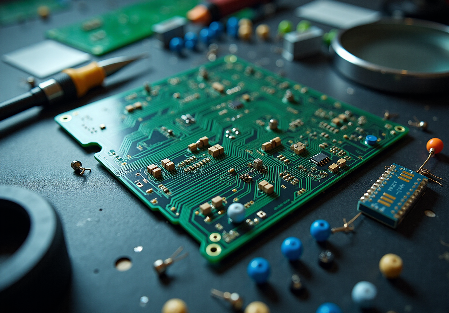
Understanding the complexities of PCB routing is essential for anyone engaged in electronic design, as it underpins the communication and functionality of devices. With technology advancing rapidly, the need for efficient and reliable circuit layouts is increasingly critical, especially in high-stakes areas such as medical equipment. As devices grow more compact and intricate, designers face the challenge of ensuring optimal performance while adhering to established guidelines. This article explores the fundamental concepts of PCB routing, its historical evolution, and the key principles that can improve both manufacturability and functionality in electronic design.
What is is the process of establishing electrical connections between various components on a . This involves outlining routes known as traces, which facilitate information transmission and power distribution across the board. Understanding what is PCB routing is essential for ensuring efficient communication, thereby minimizing delays and distortions that could adversely affect device performance.
Key terminology includes:
Understanding what is PCB routing and these terms is vital for anyone engaged in PCB design, as they lay the groundwork for how electronic circuits are constructed and operate. In the context of , can significantly impact the reliability and efficiency of the apparatus, ensuring compliance with stringent industry standards. For instance, well-designed can enhance , which is critical for the precise functioning of medical sensors and equipment. Data indicates that incorrect routing can lead to increased production costs and delays, underscoring the importance of adhering to .

plays a crucial role in electronic design, significantly impacting the performance, reliability, and manufacturability of products. Efficient pathways facilitate effective transmission between components, which is essential for maintaining transmission integrity and minimizing electromagnetic interference (EMI). In the context of , precise directing is vital; it ensures that signals from sensors are accurately conveyed to processing units, thereby preventing distortion that could compromise functionality.
, leveraging its expertise in innovative , underscores the necessity of . For instance, in a recent collaboration, Voler assisted a medical equipment firm in implementing , leading to a notable reduction in production costs and timelines, thus enhancing overall manufacturability. This partnership yielded that adhered to stringent design specifications and improved turnaround times, thereby expediting research and development processes.
As electronic devices become increasingly compact and complex, the importance of precise PCB pathways escalates. This has become a focal point for engineers and designers, as the choices made regarding pathways directly influence performance and reliability. Expert insights indicate that can significantly enhance , ensuring that equipment operates effectively in demanding environments. Consequently, investing in advanced PCB design techniques is imperative for manufacturers striving to produce high-quality, reliable medical devices.

The evolution of can be traced back to the early 20th century, marking the development of the first . Initially, the process was manual, with engineers physically connecting components using wires. The introduction of revolutionized this method, facilitating more compact and reliable designs.
Over the decades, advancements in have transformed into a more automated and efficient process. Techniques such as auto-navigation and have emerged, enabling designers to optimize layouts for both performance and manufacturability.
Today, stands as a that incorporates various strategies to meet the demands of .

Understanding what is involves several that center on key elements significantly impacting performance and manufacturability, which are crucial for ensuring in . Maintaining short and direct traces is vital for ; longer traces can introduce unwanted latency. The selection of trace width is equally critical; it must align with current requirements to prevent overheating and ensure reliable operation. For example, maintaining a distance of at least 10-15 mil from the board edges can help mitigate EMI leakage, which is essential for . Additionally, sharp corners should be avoided, as they can lead to reflections that degrade performance.
Establishing a robust ground plane beneath trace lines is essential for and minimizing . This practice supports a steady return route for data, which is vital for . Furthermore, careful placement of vias is necessary, as they can introduce inductance that negatively affects signal quality. As noted by Hi5 Electronics, ensuring adequate spacing between copper features enhances fabrication reliability and reduces the likelihood of shorts or defects.
By adhering to these , designers can not only enhance the performance of their PCBs and improve manufacturability but also understand what is , ensuring that the final product meets industry standards and customer expectations. Following these guidelines contributes to , ultimately leading to the success of engineering design projects.

In conclusion, PCB routing is a critical element of electronic design that establishes the connections among various components on a printed circuit board. The importance of effective PCB routing is paramount, as it directly impacts the performance, reliability, and manufacturability of electronic devices. A solid understanding of core concepts, including traces, vias, and pads, is essential for professionals engaged in PCB design, particularly in precision-driven industries like medical equipment.
Insights from the article reveal the evolution of PCB routing from manual methods to advanced automated techniques, highlighting the necessity of adhering to established best practices. These practices - such as maintaining short and direct traces, selecting appropriate trace widths, and minimizing electromagnetic interference - are vital for optimizing PCB layouts. By implementing these strategies, designers can enhance signal integrity and ensure compliance with industry standards, all while reducing production costs and delays.
Ultimately, the significance of PCB routing transcends mere technical specifications; it forms a foundational element for the success of electronic devices. By embracing advanced PCB design techniques and adhering to recognized best practices, engineers can not only improve product quality and efficiency but also foster innovation in an increasingly complex technological landscape. Investing in these practices is essential for achieving excellence in electronic design and manufacturing.
What is PCB routing?
PCB routing is the process of establishing electrical connections between various components on a printed circuit board (PCB) by outlining routes known as traces, which facilitate information transmission and power distribution across the board.
Why is understanding PCB routing important?
Understanding PCB routing is essential for ensuring efficient communication between components, minimizing delays and distortions that could negatively affect device performance.
What are traces in PCB routing?
Traces are the conductive paths that carry electrical signals on a printed circuit board.
What are vias in PCB routing?
Vias are the connections that allow electrical transmissions to pass between different layers of the PCB.
What are pads in PCB routing?
Pads are the areas on the PCB where components are soldered onto the board.
How does effective PCB layout impact medical equipment?
Effective PCB layout can significantly impact the reliability and efficiency of medical equipment, ensuring compliance with stringent industry standards and enhancing signal integrity for precise functioning.
What are the consequences of incorrect PCB routing?
Incorrect routing can lead to increased production costs and delays, highlighting the importance of adhering to best practices in PCB design.
Do you have a question about our services, pricing, samples, resources, or anything else?
