Introduction
Understanding the distinctions between P-type and N-type semiconductors is crucial for comprehending their significant role in modern technology, especially within the medical field. These two categories of materials possess unique electrical properties that not only influence the design of electronic components but also enhance the functionality of essential medical devices. As healthcare technology advances, the challenge lies in optimizing these semiconductors to fulfill the demands of precision and reliability. Insights derived from the differences in charge carriers and conductivity are vital, as they shape the future of medical innovations.
Define P-Type and N-Type Semiconductors
represent two fundamental categories of extrinsic substances, composed of elements doped with impurities to enhance their electrical properties.
- P-type materials are created by introducing trivalent elements, such as boron or gallium, into a pure substance like silicon. This process leads to an abundance of 'holes' or positive charge carriers, as each trivalent atom generates a vacancy for an electron.
- Conversely, N-type materials are formed by incorporating pentavalent elements, such as phosphorus or arsenic, which provide additional electrons, resulting in an excess of negative charge carriers.
is crucial in electronic physics, as these two categories exhibit different electrical behaviors and find , particularly in .

Differentiate Charge Carriers and Conductivity
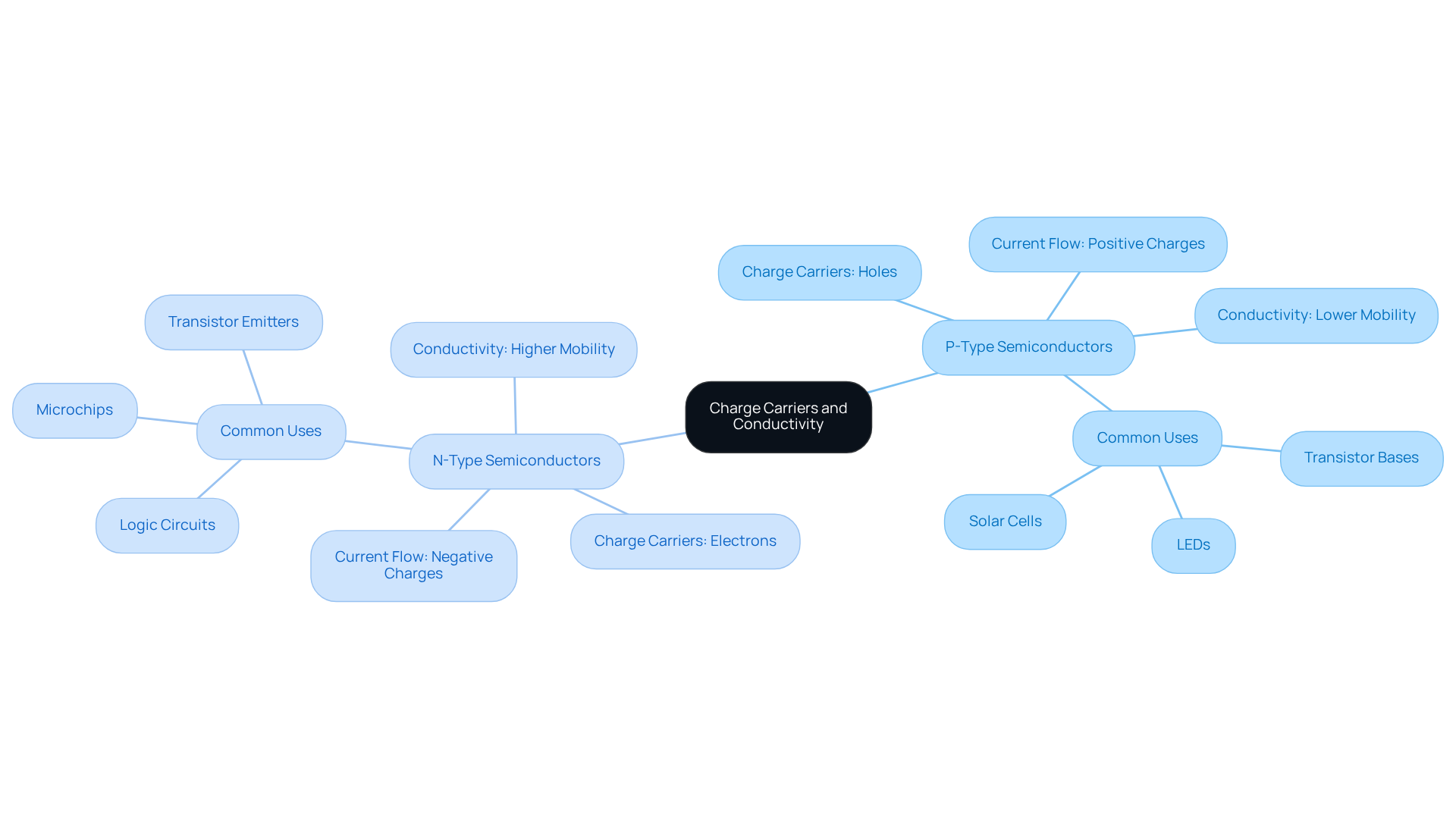
The primary distinction in the resides in their . In , which illustrates the , while electrons act as the secondary transporters. This results in by the movement of holes, which are understood as positive charges. Conversely, the is highlighted as , enhancing conductivity due to the superior mobility of these negatively charged particles. Research indicates that the p and n type semiconductor difference reveals that negatively-doped materials generally demonstrate higher conductivity compared to their positively-doped counterparts, as electrons possess greater mobility than holes.
Understanding the dynamics of charge carriers is essential for the design of in , where precise control over electrical signals is paramount. For instance, N-type materials are often preferred in applications that require high conductivity, such as in the development of advanced medical sensors and instruments, ensuring reliable performance in critical healthcare settings.
employs AI-compatible design methodologies to optimize power management in these products, extending battery life and ensuring consistent performance even under challenging conditions. The Hall effect serves as a crucial technique for verifying the type of solid-state device, as the polarity of the voltage generated by charge carriers in a magnetic field can reveal whether the majority carriers are electrons or holes.
This comprehensive understanding of chip types and their characteristics, combined with ' innovative solutions, is vital for medical equipment manufacturers aiming to enhance performance.

Explore Applications and Importance in Technology
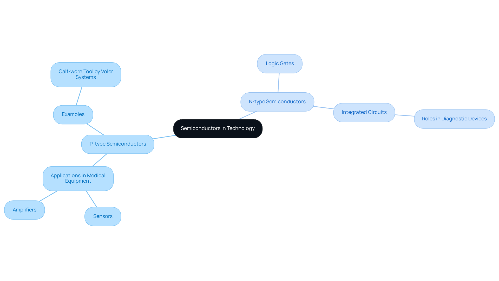
play a crucial role in the operation of various electronic instruments, particularly within the . These materials are often found in diodes and transistors, which are vital components in signal processing and amplification in medical equipment. In contrast, are essential for the construction of logic gates and integrated circuits, enabling complex calculations in diagnostic devices.
The integration of P-type and N-type materials forms p-n junctions, illustrating the , which is fundamental to the operation of instruments such as sensors, amplifiers, and microcontrollers used in wearable health monitors and imaging systems. A notable example is the innovative calf-worn tool developed by , designed to detect motion and circumference, significantly aiding in knee replacement rehabilitation. This device exemplifies how the manipulation of semiconductors enables engineers to create that adhere to stringent regulatory standards in the medical industry, ultimately enhancing patient care and outcomes.
Incorporating user testimonials could further illustrate the device's effectiveness and its impact on rehabilitation.

Conclusion
P-type and N-type semiconductors serve as essential components in electronic devices, particularly within the medical sector. Their unique properties, determined by the type of charge carriers - holes in P-type and electrons in N-type - underscore the critical differences that shape their applications. Understanding these distinctions is vital for the development of advanced medical technologies that enhance patient care and diagnostic capabilities.
Key insights indicate that P-type materials are defined by their positive charge carriers, while N-type materials demonstrate superior conductivity due to their abundance of electrons. This fundamental difference not only influences the performance of electronic components but also dictates their suitability for specific applications in medical devices, including sensors and integrated circuits. The integration of these two semiconductor types into p-n junctions is crucial for creating reliable and efficient devices that comply with stringent healthcare standards.
As semiconductor technology continues to advance, the significance of comprehending P-type and N-type materials remains paramount. Their roles in shaping the future of medical devices highlight the necessity for ongoing research and innovation. By embracing these insights, we can pave the way for next-generation healthcare solutions, ultimately enhancing patient outcomes and transforming the landscape of medical technology.
Frequently Asked Questions
What are P-type and N-type semiconductors?
P-type and N-type semiconductors are two fundamental categories of extrinsic materials that have been doped with impurities to enhance their electrical properties.
How are P-type semiconductors created?
P-type semiconductors are created by introducing trivalent elements, such as boron or gallium, into a pure substance like silicon, resulting in an abundance of 'holes' or positive charge carriers.
What elements are used to form N-type semiconductors?
N-type semiconductors are formed by incorporating pentavalent elements, such as phosphorus or arsenic, which provide additional electrons and create an excess of negative charge carriers.
Why is it important to understand the difference between P-type and N-type semiconductors?
Understanding the difference between P-type and N-type semiconductors is crucial in electronic physics because they exhibit different electrical behaviors and are used in various applications, particularly in medical devices.
List of Sources
- Differentiate Charge Carriers and Conductivity
- What are P type and N type Silicon Wafers? | WaferPro (https://waferpro.com/what-are-p-type-and-n-type-silicon-wafers?srsltid=AfmBOorjfiZpcQrl2RqN9xbsakHoyQ_lpcNgXWl6t8Bh8yhM90uIFhd0)
- What is the method to differentiate between a p-type and an n-type semiconductor? | ResearchGate (https://researchgate.net/post/What-is-the-method-to-differentiate-between-a-p-type-and-an-n-type-semiconductor)
- Semiconductor Types: A Guide to Intrinsic, Extrinsic & P-N Types (https://agsdevices.com/semiconductor-types)
- aemdeposition.com (https://aemdeposition.com/blog/n-type-vs-p-type-semiconductor.html)