N-Type vs P-Type Semiconductor: Key Differences and Applications
Discover the essential differences and applications of n-type and p-type semiconductors.


Understanding the complex world of semiconductors reveals a significant duality between N-Type and P-Type materials, both essential in the field of electronics. These two categories, characterized by their distinct charge carriers and doping processes, not only impact the performance of everyday devices but also propel advancements in cutting-edge technologies, particularly within medical applications. As the demand for faster and more efficient electronic systems continues to rise, it is crucial to explore how these seemingly opposite materials collaborate to address the challenges of modern innovation.
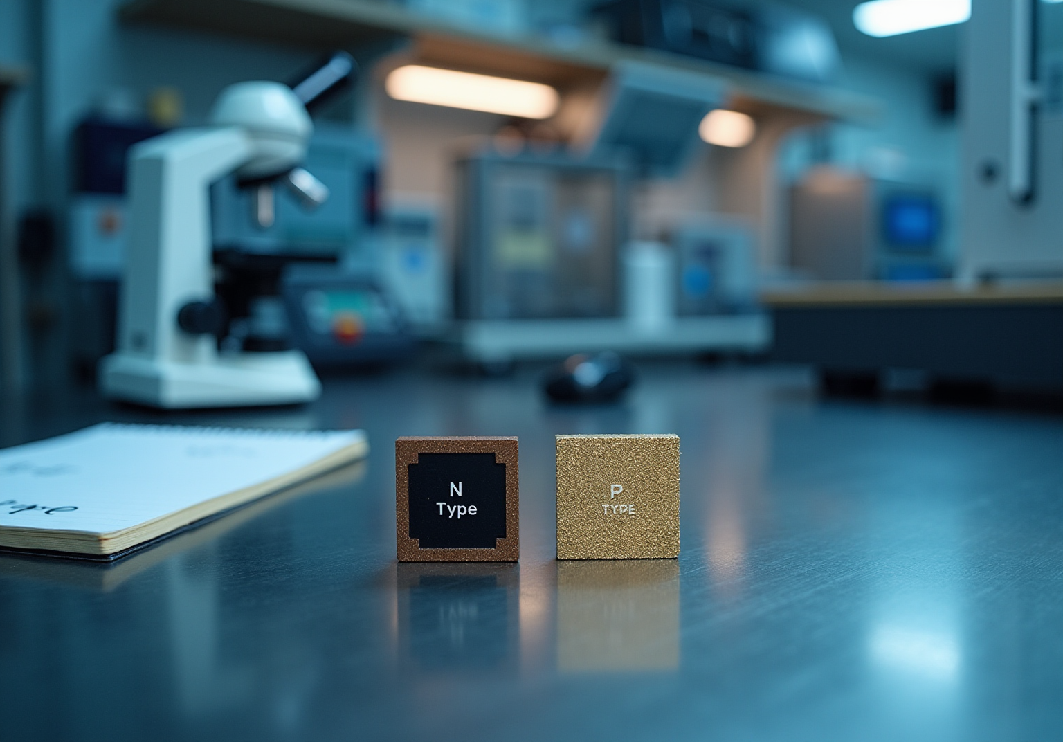
N-Channel and P-Channel types are essential categories of extrinsic materials, enhanced through doping with specific impurities to improve their electrical characteristics. An N-Type extrinsic conductor is formed by adding a dopant with more valence electrons than the base material, typically a group V element such as phosphorus. This process results in an abundance of electrons, which serve as the . Conversely, a P-Type material is created by doping with a trivalent element, such as boron, leading to the formation of 'holes' or vacancies where electrons can reside, making these holes the predominant . The designations 'N' and 'P' reflect the negative and positive , respectively, emphasizing the difference between and in their distinct charge transport mechanisms.
In contemporary electronic equipment, are often preferred due to their superior electron mobility, which enhances performance in applications such as transistors and diodes. Recent research indicates that certain materials constitute a significant share of electronic component usage, particularly in high-speed and high-power applications. In healthcare devices, are utilized in advanced sensors and diagnostic tools, while play a crucial role in developing efficient power management systems. leverages these chip technologies to extend battery life in wireless medical devices by implementing strategies such as limiting transmission power, utilizing low-power sensors, and optimizing energy consumption through . As the microelectronics sector continues to evolve, ongoing research is dedicated to exploring innovative applications and enhancements in both N and P materials, ensuring their relevance in the rapidly advancing technological landscape.

The movement of electrons in N-Type materials illustrates the difference between , as electrons serve as the primary charge carriers. When a voltage is applied, these excess electrons migrate toward the positive terminal, generating an . This abundance of free electrons significantly improves the material's conductivity.
The is that P-Type materials operate through the , which represent the absence of electrons in the valence band. Upon applying voltage, electrons from the valence band can leap into these holes, allowing the holes to shift toward the negative terminal. This signifies the current flow in P-Type materials.
The interaction between negative and positive between , which are crucial for forming . Recent advancements in chip technology have focused on enhancing charge carrier mobility. Experts have noted that .

The is fundamental to a wide range of electronic applications, especially in the . The is evident in N-Type materials, which are characterized by their abundance of electrons and are widely utilized in the production of transistors, diodes, and integrated circuits. Their superior electrical conductivity renders them ideal for the fabrication of logic gates and amplifiers, which are crucial components in numerous electronic systems. For example, , enabling precise monitoring and diagnostics.
Conversely, the is that , which are essential for the operation of diodes and solar cells. Recent advancements have led to the , such as wearable tools designed for tracking movement and circumference during knee replacement recovery. These devices not only ensure compliance with medical equipment standards but also provide critical information for patient recovery, illustrating the practical applications of these components in real-world scenarios.
The collaboration between N-Type and P-Type materials illustrates the , supporting the functionality of everyday electronics, such as smartphones and laptops, while also underpinning essential medical equipment. Their combined capabilities are crucial for the development of innovative technologies in the , where . As the demand for intelligent continues to rise, the role of these components in ensuring reliable performance and adherence to stringent industry standards becomes increasingly significant. Furthermore, underscore the importance of these materials in enhancing patient care and outcomes. Understanding the is essential for driving future technological innovations, as emphasized by expert Donald A. Neamen, highlighting the importance of this knowledge in the field of .

The fundamental difference between is based on their . , which serve as the primary charge carriers. In contrast, , making them the main charge carriers. The doping elements also vary significantly: n-type materials are typically doped with pentavalent elements from Group V of the periodic table, such as phosphorus or arsenic, while p-type materials are infused with trivalent elements from Group III, like boron or aluminum. Notably, phosphorus-doped silicon can achieve a solubility limit of approximately 1.5 × 10^21 atoms/cm^3 at 1100°C, whereas antimony has a solubility limit of around 7 × 10^20 atoms/cm^3 at the same temperature. Understanding this information is crucial for grasping the and its effects on .
In terms of , n-type materials typically exhibit compared to their p-type counterparts. The Fermi level in n-type materials is positioned closer to the conduction band, which enhances their electrical characteristics. Conversely, in p-type materials, the Fermi level is situated between the energy level of the acceptor and the valence band. This improved conductivity is vital for , such as high-speed transistors and diodes. Recent studies have highlighted that n-type materials can achieve greater operational efficiencies in applications like solar cells and LEDs, where swift electron movement is essential for optimal .
Understanding the difference between is critical for engineers and designers engaged in chip technology, as their choice can significantly influence the and efficiency of . The interaction between these two types of semiconductors is foundational to the advancement of modern electronics, affecting everything from microprocessors to .

N-Type and P-Type semiconductors are foundational components of modern electronics, each serving a distinct role defined by their charge carriers and electrical properties. N-Type semiconductors, characterized by an abundance of electrons, excel in conductivity and are pivotal in applications that require rapid charge transport. In contrast, P-Type semiconductors, which feature holes as their primary charge carriers, are essential for creating P-N junctions and are widely utilized in various electronic devices.
Key distinctions between these semiconductor types have emerged throughout this exploration:
The interplay between these two types is vital for the functionality of many electronic systems, underscoring their complementary roles in technology.
Understanding the differences between N-Type and P-Type semiconductors extends beyond academic curiosity; it is essential for engineers and designers aiming to innovate in the rapidly advancing field of electronics. As the demand for efficient and intelligent devices grows, the continued exploration and application of these semiconductor technologies will be key to driving progress in industries ranging from healthcare to consumer electronics. Embracing this knowledge not only enhances device performance but also paves the way for future advancements in technology.
What are N-Type and P-Type semiconductors?
N-Type and P-Type semiconductors are categories of extrinsic materials that have improved electrical characteristics due to doping with specific impurities. N-Type semiconductors have an abundance of electrons as charge carriers, while P-Type semiconductors have 'holes' or vacancies that serve as the predominant charge carriers.
How is an N-Type semiconductor formed?
An N-Type semiconductor is formed by doping a base material with a dopant that has more valence electrons, typically a group V element like phosphorus. This results in an excess of electrons, which are the majority charge carriers.
What creates a P-Type semiconductor?
A P-Type semiconductor is created by doping a base material with a trivalent element, such as boron. This process leads to the formation of holes where electrons can reside, making these holes the predominant charge carriers.
What do the designations 'N' and 'P' signify?
The designations 'N' and 'P' reflect the type of charge carriers in the semiconductors, with 'N' indicating negative charge carriers (electrons) and 'P' indicating positive charge carriers (holes).
Why are N-Type materials often preferred in electronic equipment?
N-Type materials are often preferred due to their superior electron mobility, which enhances performance in applications like transistors and diodes.
In what applications are N-Type materials used?
N-Type materials are used in high-speed and high-power applications, as well as in advanced sensors and diagnostic tools in healthcare devices.
What role do P-Type materials play in technology?
P-Type materials are crucial for developing efficient power management systems in various electronic applications.
How does Voler Systems utilize N-Type and P-Type technologies?
Voler Systems leverages N-Type and P-Type chip technologies to extend battery life in wireless medical devices by implementing strategies such as limiting transmission power and optimizing energy consumption through AI-driven power management solutions.
What is the focus of ongoing research in the field of semiconductors?
Ongoing research is dedicated to exploring innovative applications and enhancements in both N-Type and P-Type materials to ensure their relevance in the rapidly advancing technological landscape.
Do you have a question about our services, pricing, samples, resources, or anything else?
