Get Help On Your Device Design

PCB Layout Checklist

post_banner

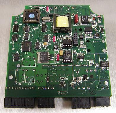
When we do printed circuit board (PCB) design we check all of the items in this PCB Layout Checklist and more. Some of the items in the list are general guidelines and we often  need to use engineering judgment on the trade-off between the size, cost, testability, and manufacturability of the board. Note: This checklist was influenced by an earlier checklist put together by Hank Wallace. See http://www.aqdi.com/check.htm for his current version.

PCB Layout Checklist
Part Placement
  1. SMD component orientation consistent
  2. clearance for IC extraction tools
  3. all polarized components checked
  4. place thruhole components on 50 mil grid
  5. check the orientation of all connectors
  6. minimum component body spacing
  7. bypass capacitors located close to IC power pins
  8. verify that all series terminators are located near the source
  9. I/O drivers near where their signals leave the board
  10. PCB has ground turrets, power rail test points, and test points for important signals, all labeled
  11. EMI and RFI filtering as close as possible to exit and entry points in shielded areas
  12. layout PCB so that any rework or repair of a component does not require removal of other components
  13. potentiometers should increase controlled quantity clockwise
  14. mounting holes electrically isolated or not
  15. proper mounting hole clearance for hardware
  16. SMD pad shapes checked
  17. tooling holes for automated assembly
  18. sufficient clearance for socketed ICs
  Routing
  1. digital and analog signal commons joined at only one point
  2. check for traces running under noisy or sensitive components
  3. no vias under metal-film resistors and similar poorly insulated parts
  4. check for traces which may be susceptible to solder bridging
  5. check for dead-end traces, unless used on purpose
  6. ensure schematic software did / did not separate Vcc from Vdd, Vss from GND as needed
  7. provide multiple vias for high current and/or low impedance traces
  8. component and trace keepout areas observed
  9. ground planes where possible
  Dimensions
  1. hole diameter on drawing are finished sizes, after plating.
  2. finished hole sizes are >=10 mils larger than lead
  3. silkscreen legend text weight >=10 mils
  4. pads >=15 mils larger than finished hole sizes
  5. components >=0.2″ from edge of PCB
  6. test pads 200 mils from edge of board
  Dimensions cont.
  1. traces >= 20 mils from edge of PCB
  2. thru-hole drill tolerance noted
  3. thru-hole soldermask tolerance noted
  4. thru-hole route tolerance noted
  5. thru-hole silkscreen legend tolerance noted
  6. trace width sufficient for current carried
  7. sufficient clearance for high voltage traces
Silk Screen
  1. no silkscreen legend text over vias (if vias not soldermasked) or holes
  2. all legend text reads in one or two directions
  3. company logo in silkscreen legend
  4. company logo in foil
  5. copyright notice on PCB
  6. date code on PCB
  7. PCB part number on PCB
  8. assembly part number on PCB
  9. PCB revision on silkscreen legend
  10. assembly revision blank on silkscreen legend
  11. serial number blank on silkscreen legend
  12. all silkscreen text located to be readable when the board is populated
  13. all ICs have pin one clearly marked, visible even when chip is installed
  14. high pin count ICs and connectors have corner pins numbered for ease of location
  15. silk screen tick marks for every 5th or 10th pin on high pin count ICs and connectors
Other
  1. CAD design rule checking must be turned on
  2. high frequency circuitry precautions observed
  3. extra connector and IC pins accessible on prototype boards, just in case
  4. check hole diameters for odd components: rectangular pins, spring pins
  5. soldermask does or does not cover vias
  6. no acute inside angles in foil
  7. soldermask swell checked
  8. manual netlist check
  9. check netlist for nodes with only one connection
  10. drill origin is a tooling hole
  11. PCB thickness, material, copper weight noted
  12. thermal reliefs for internal power layers
  13. solder paste mask openings are proper size
  14. blind and buried vias allowed on multilayer PCB
  15. PCB layout panelized correctly
  16. high frequency crystal cases should be flush to the PCB and grounded

Highly Successful Engineering Design Projects

Other Useful PCB Layout Checklist Tools and Documents

Other Voler Checklists and Design Guides

Share:

TELL US ABOUT YOUR NEXT DESIGN PROJECT

Do you have a question about our services, pricing, samples, resources, or anything else?

Contact Us Now

Related News

Risk Management For Component Selection | Voler Systems

Voler provided component selection and evaluation, prototype and production board design...

Read More

Walt Maclay Selected as Reviewer for SBIR/STTR Programs

Walt Maclay is honored to be selected as a reviewer for the National Science Foundation’s...

Read More

Product Development & Management Tips | Voler Systems

Managing product development is difficult. Especially when you don’t have a technology...

Read More

Interested in Learning More? Contact Us Today!