What Are The Best Heart Rate Monitors of 2021 | Voler Systems
The proliferation of fitness bands and smartwatches has made us more fitness-conscious,...

The rapid evolution of technology has significantly transformed the landscape of electronic design, rendering Electronic Design Automation (EDA) tools essential for the creation of complex integrated circuits. These robust applications not only streamline the design process but also enhance productivity and accuracy, enabling engineers to navigate the complexities of Very Large Scale Integration (VLSI) with greater ease. As the demand for increasingly sophisticated electronic systems continues to rise, it becomes imperative for designers to ensure they are fully leveraging the capabilities of EDA tools to address contemporary challenges.
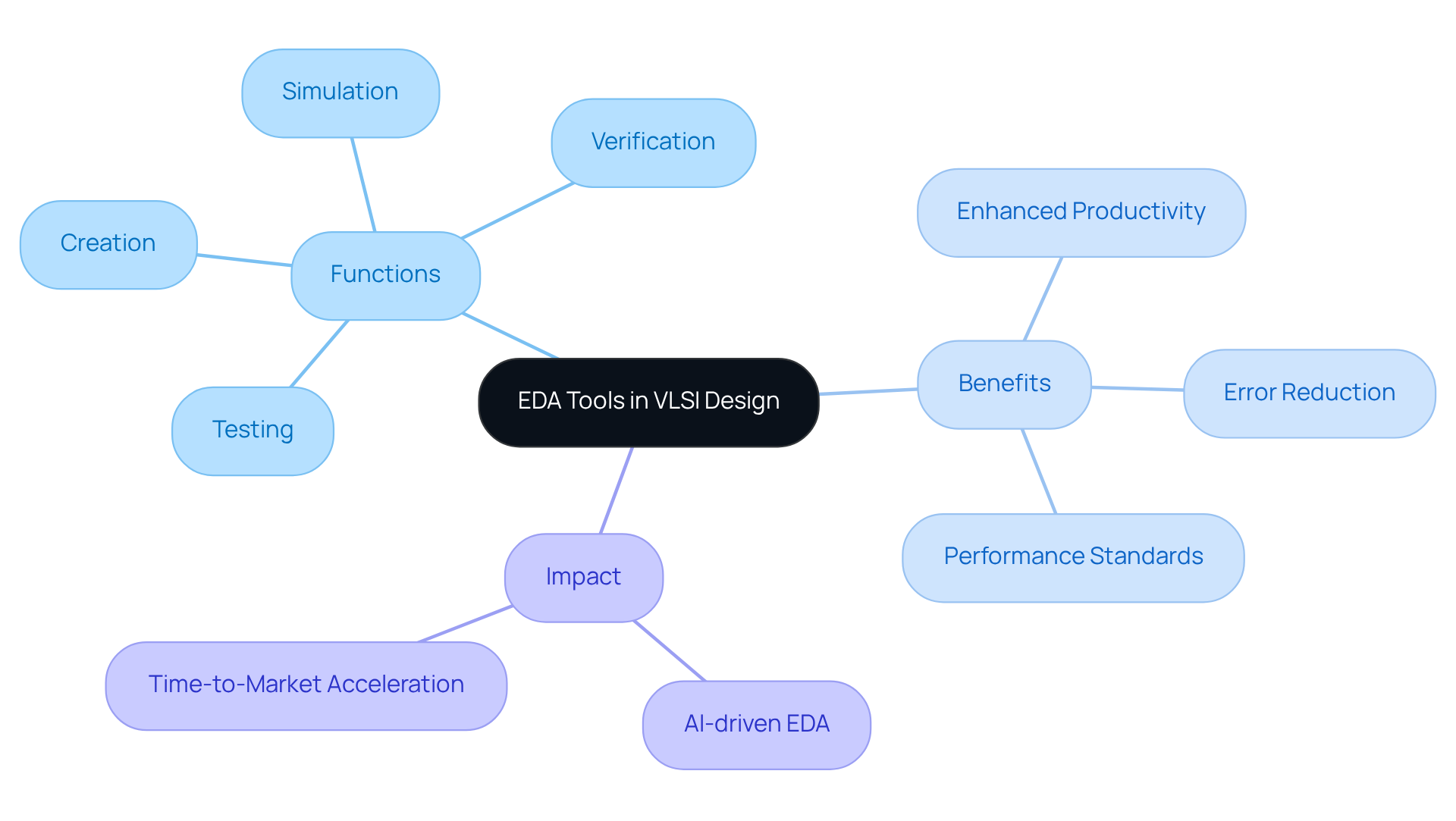
applications are essential software tools that streamline the creation, simulation, verification, and testing of electronic systems, particularly integrated circuits (ICs) and . These tools automate complex es, allowing engineers to efficiently produce advanced electronic components.
In the realm of development, the use of EDA tools for VLSI is indispensable, managing the intricacies of circuits that may comprise over a billion components. Their importance is underscored by their ability to .
For instance, can , significantly accelerating the time-to-market for new products. Furthermore, these tools provide , enabling designers to evaluate multiple architectural variants concurrently.
Without EDA resources, the would be considerably slower and more susceptible to errors, underscoring their .

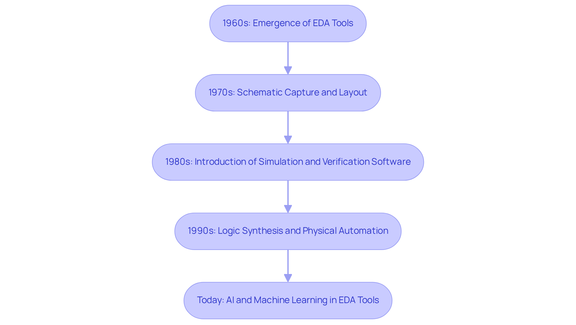
The development of began in the 1960s, coinciding with the emergence of integrated components that necessitated more efficient creation methods than traditional manual drafting. Early EDA applications focused on schematic capture and layout, enabling engineers to automate the creation of diagrams. A significant advancement occurred in the 1980s with the introduction of simulation and verification software, which allowed designers to test circuits virtually before physical implementation. As the 1990s approached, EDA applications evolved further, incorporating advanced features such as logic synthesis and physical automation.
Today, the use of leverages cutting-edge technologies, including artificial intelligence and machine learning, to optimize processes, enhance accuracy, and significantly reduce time-to-market. Companies like exemplify this trend by employing in their embedded systems and FPGA designs, particularly for . Their focus on improving involves strategies such as:
This approach addresses critical challenges in .
This historical overview underscores the continuous innovation within , highlighting the increasing complexity of electronic systems and the pressing need for more efficient development methodologies.

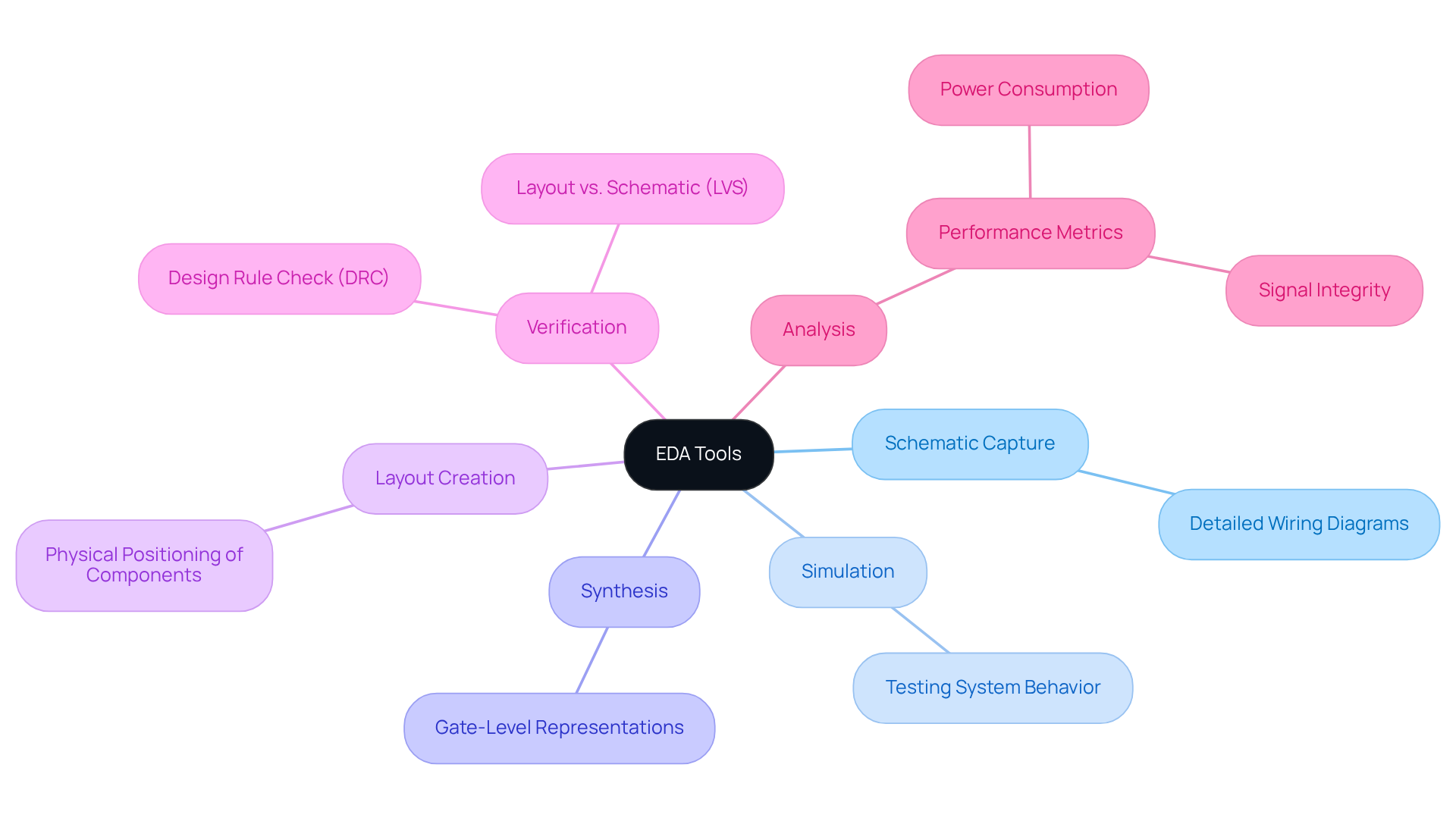
EDA applications are essential for optimizing the , offering a range of critical features. Among these functionalities is schematic capture, which enables engineers to develop detailed wiring diagrams. Simulation allows for testing system behavior under various conditions, while synthesis transforms high-level descriptions into gate-level representations. Furthermore, EDA software facilitates layout creation, ensuring the accurate physical positioning of components on a printed circuit board (PCB).
Verification resources, such as and Layout vs. Schematic (LVS), are vital for confirming that layouts meet specified requirements and industry standards. Analysis tools assess performance metrics, including power consumption and . The integration of these features into a cohesive workflow empowers engineers to iterate swiftly, identify potential issues early in the design phase, and refine models for manufacturability and performance.
This comprehensive functionality underscores the critical role of in the development landscape, especially as the industry shifts towards more complex architectures like chiplets and 3D ICs, where traditional methods may fall short. At , we harness to enhance these processes, especially in the development of efficient wireless medical devices. Our expertise in FPGA development allows us to improve , ensuring reliable performance in demanding applications. This integration of advanced EDA resources, including targeted verification and analysis functionalities, along with AI capabilities, positions as a leader in delivering high-performance solutions tailored to the needs of medical device manufacturers.

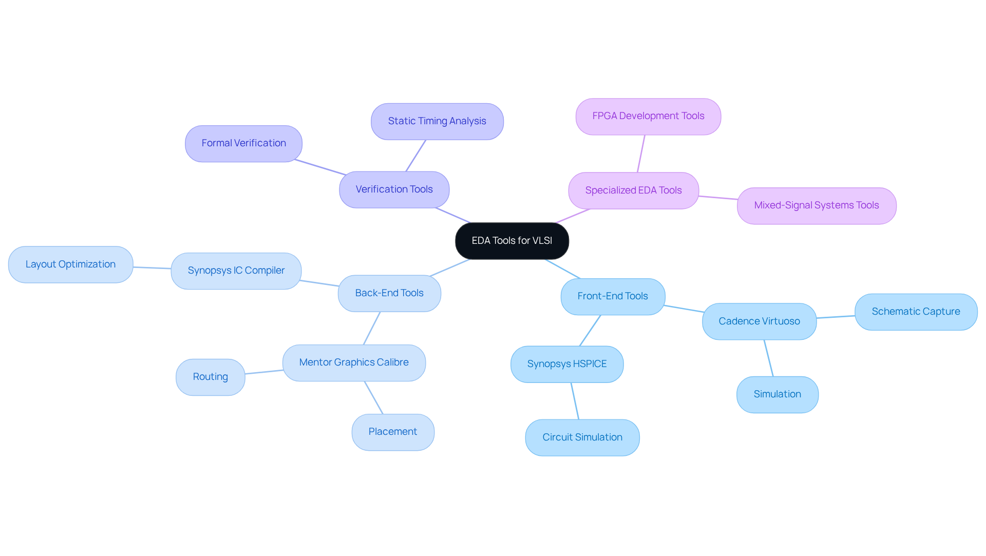
The creation and development of integrated systems heavily rely on , which are categorized by their specific functions. , including Cadence Virtuoso and Synopsys HSPICE, are indispensable for schematic capture and simulation. These enable engineers to efficiently develop and evaluate , ensuring the feasibility of initial concepts before advancing to subsequent development phases.
Conversely, focus on the and layout of chips. , including Mentor Graphics' Calibre and Synopsys' IC Compiler, are vital for placing and routing components on a chip, optimizing layouts for manufacturability and performance. , including formal verification and static timing analysis, are also integral to the EDA process, confirming that designs meet both functional and .
Additionally, specialized cater to specific applications, such as FPGA development and mixed-signal systems, further enriching the ecosystem. By 2026, the market share of various EDA solutions illustrates the competitive landscape, with leading companies like Synopsys, Cadence, and Siemens EDA dominating the sector. A clear understanding of the distinctions between front-end and back-end tools, along with their respective applications, empowers engineers to select the most appropriate for their design challenges, ultimately enhancing the efficiency and success of .

The significance of Electronic Design Automation (EDA) tools in VLSI design is paramount. These sophisticated applications form the backbone of modern electronic engineering, streamlining the design, simulation, and testing processes of integrated circuits and printed circuit boards. By automating complex tasks, EDA tools enhance productivity and minimize errors, ensuring that designs adhere to rigorous industry standards.
This article has traced the evolution of EDA tools from their inception in the 1960s to their current state, which incorporates advanced technologies such as artificial intelligence. Key features, including schematic capture, simulation, and verification, play a crucial role in facilitating efficient design workflows. The differentiation between front-end and back-end tools underscores their specific applications, empowering engineers to select the appropriate resources for their unique challenges.
In conclusion, as the complexity of electronic systems continues to escalate, the relevance of EDA tools for VLSI design becomes increasingly critical. Their capacity to optimize development processes not only accelerates time-to-market but also fosters innovation across various sectors, including medical devices and consumer electronics. Embracing these tools is essential for any organization striving to excel in the competitive landscape of electronic design, reinforcing the notion that the future of engineering lies in the seamless integration of advanced technologies and efficient methodologies.
What are EDA tools?
EDA tools, or Electronic Design Automation tools, are essential software applications that streamline the creation, simulation, verification, and testing of electronic systems, particularly integrated circuits (ICs) and printed circuit boards (PCBs).
Why are EDA tools important in VLSI design?
EDA tools are crucial in VLSI design because they manage the complexities of circuits that can contain over a billion components, enhancing productivity, reducing errors, and ensuring compliance with performance and manufacturing standards.
How do EDA tools improve the development process?
EDA tools automate complex development processes, allowing engineers to produce advanced electronic components more efficiently. They also provide real-time feedback and optimization, enabling designers to evaluate multiple architectural variants simultaneously.
What impact do AI-driven EDA tools have on product development?
AI-driven EDA tools can significantly accelerate the development process, compressing months of work into weeks, which helps to speed up the time-to-market for new products.
What would happen without EDA resources in electronic engineering?
Without EDA resources, the development process would be considerably slower and more prone to errors, highlighting their critical role in modern electronic engineering.
