Best Practices for Layout PCB Design in Medical Devices
Explore best practices for layout PCB design in medical devices to ensure reliability and...


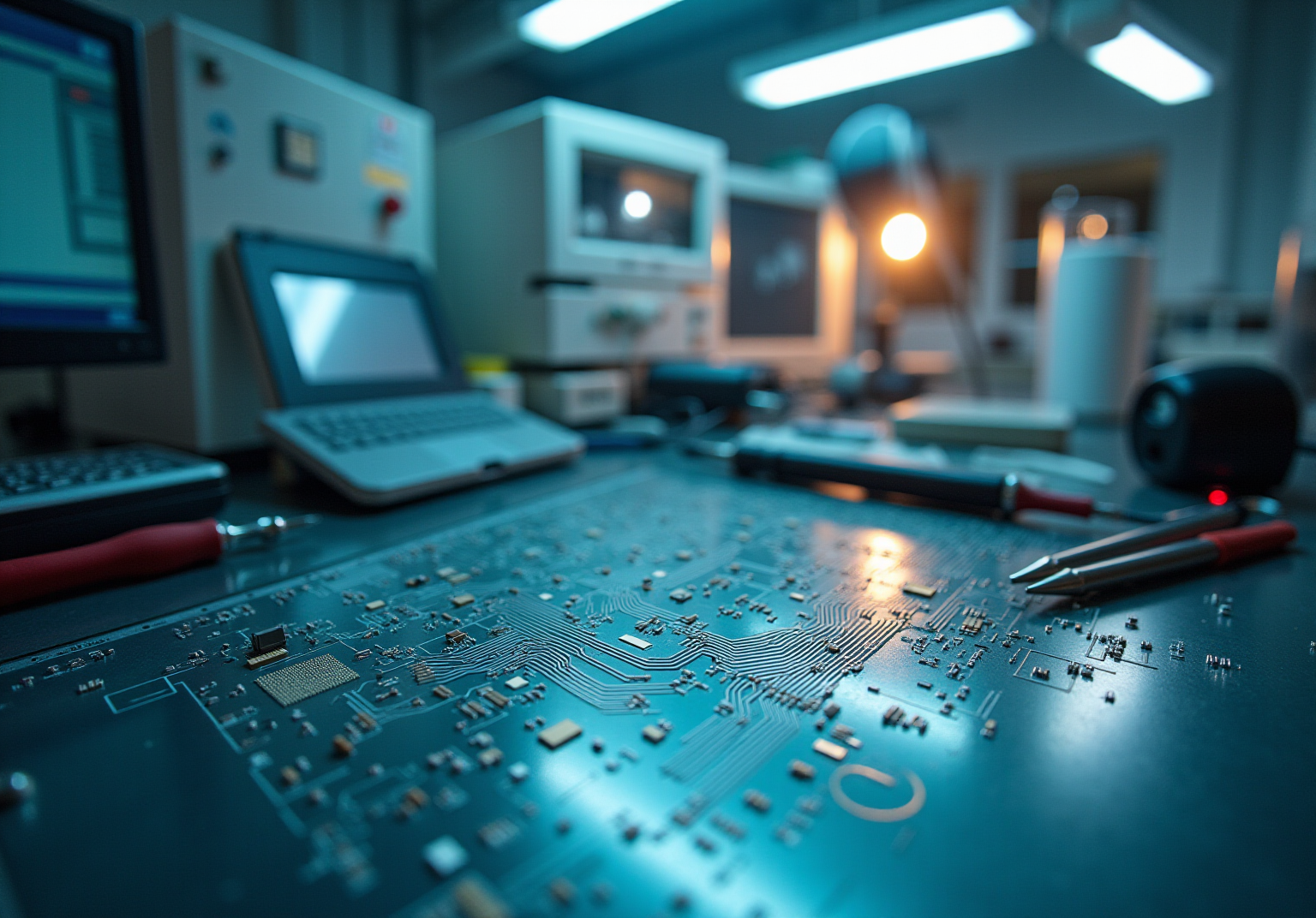
High-frequency printed circuit boards (PCBs) are crucial in modern electronics, particularly in the medical device sector, where precision and reliability are essential. These specialized boards, engineered to function at frequencies exceeding 1 GHz, are vital for ensuring efficient data transmission and preserving signal integrity in critical applications.
However, mastering high-frequency PCB design presents numerous challenges, ranging from material selection to impedance control. How can engineers effectively navigate these complexities to develop safe, efficient, and innovative healthcare solutions?
are engineered to operate at frequencies exceeding 1 GHz, which is essential for high-speed data transmission with minimal loss and distortion. Their key characteristics include:
Understanding these characteristics is essential for engineers involved in the development of health-related devices, as they directly impact the safety, effectiveness, and being created. With ' extensive experience in developing class III health devices and the integration of , manufacturers can expedite the creation of , ensuring they meet the evolving demands of modern healthcare.

Designing a necessitates meticulous attention to several critical factors that directly influence performance and reliability, particularly in .
By carefully evaluating these design components, engineers can develop that not only meet the stringent requirements of the healthcare device sector but also ensure reliable and efficient performance in critical applications.

, highlighting their versatility and significance in technological advancement. In the healthcare devices sector, these boards are essential for:
These applications facilitate . For example, has created an innovative calf-worn device aimed at detecting motion and circumference, specifically designed for knee replacement rehabilitation. is vital for these medical-grade printed circuit boards, ensuring safety and effectiveness within healthcare environments. Furthermore, utilizes to optimize battery life, thereby enhancing the performance of wireless medical devices even under challenging conditions.
In telecommunications, high frequency PCBs are indispensable for the deployment of 5G networks and satellite communications, enabling rapid data transfer and robust connectivity. The market for advanced circuit boards in telecommunications is experiencing significant growth, driven by the increasing demand for faster and more reliable communication technologies.
The aerospace and defense sectors also heavily rely on high frequency PCBs, particularly in radar systems and communication devices, where performance and reliability are paramount. These applications necessitate the highest standards of precision and durability, often conforming to stringent industry regulations.
In consumer electronics, are integral to smartphones and other advanced devices, facilitating features such as high-speed internet access and real-time data processing. This integration not only but also propels innovation in product development.
In summary, understanding the diverse applications of emphasizes their critical role in the evolution of innovative technology across multiple sectors.

Selecting appropriate materials for is crucial for optimizing performance, especially in where . The key materials include:
Careful selection of these materials ensures that maintain optimal performance in challenging environments, particularly within the medical sector, where adherence to stringent safety and efficacy standards is critical.

High-frequency PCBs play a crucial role in the advancement of medical device technology, facilitating essential applications that require high-speed data transmission with minimal signal loss. Their intricate design, characterized by low loss, impedance control, and specialized material selection, ensures that these circuit boards adhere to the stringent standards of reliability and safety that are vital in healthcare settings. A thorough understanding of these fundamental aspects is essential for engineers aiming to innovate within this sector.
This article has examined key considerations in the design of high-frequency PCBs, including:
Each of these factors significantly enhances signal integrity and reduces electromagnetic interference, ultimately improving the overall performance of medical devices. Furthermore, the choice of appropriate materials, such as PTFE and ceramic-filled substrates, highlights the necessity of optimizing PCB functionality for demanding applications.
The impact of high-frequency PCBs extends beyond the medical field, influencing telecommunications, aerospace, and consumer electronics. As the demand for faster and more reliable technology continues to escalate, the importance of these advanced circuit boards becomes increasingly evident. Adopting best practices in high-frequency PCB design and material selection not only drives innovation but also ensures that devices can effectively address the evolving challenges of modern healthcare and beyond. Engaging with these insights empowers professionals to make meaningful contributions to the future of technology in critical sectors.
What defines high-frequency PCBs?
High-frequency PCBs are engineered to operate at frequencies exceeding 1 GHz, which is essential for high-speed data transmission with minimal loss and distortion.
What are the key characteristics of high-frequency PCBs?
The key characteristics include low loss, impedance control, and careful material selection.
Why is low loss important in high-frequency PCBs?
Low loss is crucial for maintaining signal integrity in communication systems, especially in medical devices where reliability is paramount.
What is impedance control in high-frequency PCBs?
Impedance control ensures consistent impedance, preventing reflections that can disrupt signal transmission, which is vital for wearable and IoT health solutions.
What materials are commonly used in high-frequency PCBs?
Common materials include PTFE and ceramic-filled substrates, which have low dielectric constants and loss factors, enhancing performance and battery life of wireless healthcare devices.
Why is understanding high-frequency PCB characteristics important for engineers?
Understanding these characteristics is essential for engineers developing health-related devices, as they directly impact safety, effectiveness, and regulatory compliance of the products.
How does Voler Systems contribute to the development of high-frequency PCBs?
Voler Systems has extensive experience in developing class III health devices and uses AI-assisted engineering to help manufacturers create high-quality health products that meet modern healthcare demands.
Do you have a question about our services, pricing, samples, resources, or anything else?
